BACKSIDE ILLUMINATION (BSI) SERVICES
Alacron, Inc. is capable of processing sensor wafers to produce backside illuminated wafers or sensors on a contract basis. Backside illumination is performed to allow the sensor to be illuminated on the side opposite the electronics of the sensor.resulting in significantly increased quantum efficiency. This allows increased light sensitivity or reduced pixel pitch.
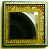
TYPICAL SILICON CMOS OR CCD SENSOR
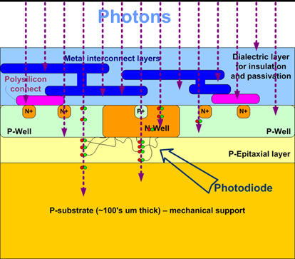
A typical image sensor such as the CMOS sensor pictured below has the electronics layers overlaying part of the pixel area. Photons entering the sensor are thus blocked by the structures overlying the photocathode as well as the associated electronics in the pixel well. This results in the reduction of photon conversion efficiency with the resultant decrease in quantum efficiency.
HANDLE WAFER PROCESSING
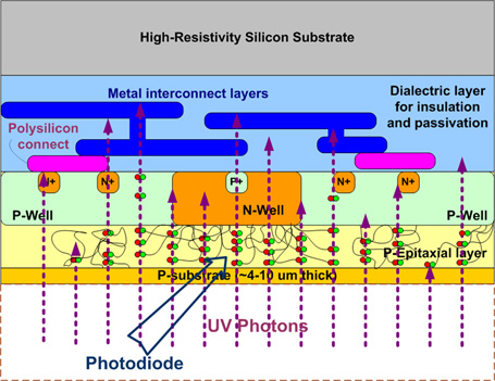
To achieve backside illumination a silicon substrate is bonded to the front side of the sensor wafer.

BACK THINNING AND ILLUMINATION
Then the backside of the sensor wafer is optionally thinned and an optionally anti-reflective coating is applied and the sensor is mounted upside down. Then the photocathode well is directly exposed to photo-electrons and no photo-electrons are thus blocked by the associated overlying electronics. This and lateral capture results in significantly increased quantum efficiency.
Click here to download presentation